GaAs – A Compound Semiconductor
Gallium arsenide is a compound semiconductor which may be defined as a semiconductor made of a compound of two elements (as opposed to silicon, which is a single element semiconductor).
The figure below shows the arrangement of atoms in a gallium arsenide substrate material. Note the alternate positioning of gallium and arsenic atoms in their exact crystallographic locations. Since gallium arsenide is a binary semiconductor special care is required during the processing to avoid high temperatures that could result in dissociation of the surface, this being one of the basic difficulties in the growth of GaAs bulk material.

GaAs Atom Arrangement
GaAs Doping Process
Much as it is with silicon, it is necessary to introduce impurities into the semi insulating Ga As material in order to facilitate the creation of switching devices Selection of the impurity and its concentration density determine the behaviour of the switching clement. According to the dopant used, both n-type and p-type material can be realized.
- n-type material
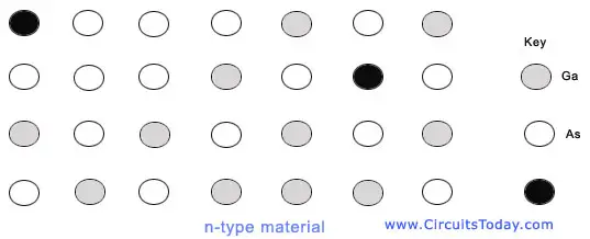
Group IV elements such as silicon can act as either donors (that is, on Ga sites) or acceptors (that is, on As sites). Since arsenic is smaller than gallium and silicon (the covalent radius for Ga is 1.26 A and for As is 1.18 A), group IV impurities tend to occupy gallium sites. Thus, silicon is used as the dopant for the formation of n-type material as shown in the figure below.
The shrinkage of atomic radii across a given row of the periodic table can best be explained by noting that in any given period, electrons are added to s and p orbitals, which are not able to shield each other effectively from the increasing positive nuclear charge. Thus an increase in the positive charge of the nucleus results in an increase in the effective nuclear charge, thereby decreasing the effective, atomic radius. This is why, for example, an As atom is smaller than a Ga atom.

n-type material
- p-type material
Beryllium (Be) or magnesium (group II) can be used for the formation of p-type material. Since Be is the lightest p-type dopant for GaAs, deep implantation of the dopant atoms can be accompiished with relatively less lattice damage. Nevertheless, Mg is also finding its way as a suitable dopant in a number of processes.
No comments:
Post a Comment